A state of frenzy arose in the Scientific World, with the discovery of graphene in 2004. Graphene, popularly known as “The Wonder Material”, held a promising potential owing to the exotic properties it displays. Graphene is a single layer of carbon atom arranged in a hexagonal honeycomb pattern.
Graphene can theoretically do anything , but move out of the lab.
Anonymous
Using graphene, researchers are now one step closer to uncover the mysteries surrounding Strongly-Correlated materials. These are a wide class of heavy fermions compounds that show exceptional electronic and magnetic properties. Properties include metal-insulator transitions, half-metallicity, and spin-charge separation which are explained by the behavior of e¯s or spinons. So far ultra-cold atom lattices were used to stimulate quantum materials.
The Exotic Phenomenon
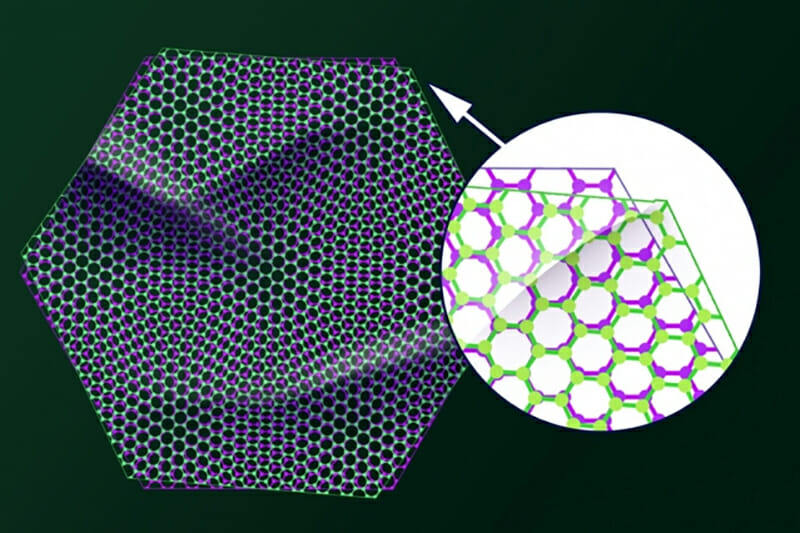
In 2018, Scientist Pablo Jarillo-Herrero and ‘Yuan Cao’ discovered an exceptional phenomenon that involves our two favorites words: Graphene and Superconductor. The team stacked two layers of graphene at a slightly offset angle, the ‘twisted graphene’ became either an insulator or theoretically a super-conductor. Angle 1.1° was among the first of the angles at which these exotic properties were observed and was coined as “Magic Angle”, while the system was coined as “Magic Angle Twisted Bi-Layer Graphene”(MA-TBG). Not only this but the research leads to the birth of a new field called “Twistronics”.
About Mott Insulators
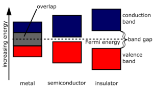
We all know that the “Band Theory” explains the concept of conduction through conduction and valence bands. In a metal, these overlap while in an insulator they have a gap called “Band-Gap”. These Bands or DOS is a mathematical equation that gives us the number of quantum states that an e¯ inside a solid metal can take. The main twist occurs when you have exactly a half-filled band(HFB) in metal, and you expect to see similar properties but instead, it behaves like an insulator. These type of insulators that should behave as a metal but aren’t, are called “Mott-Insulators”.

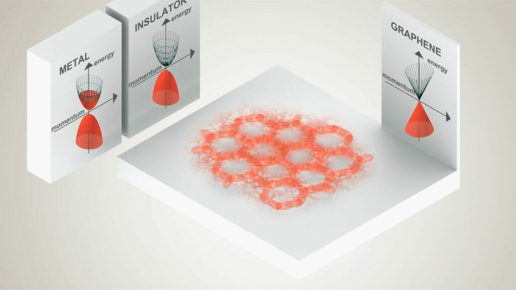
Band Energy diagrams of different materials. 
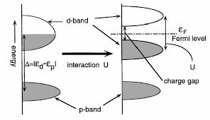
Band Energy diagram of Mott insulator showing anomaly at half-filled state.
When a metal has an exactly HFB, the e¯ should be able to move from one atom to another but the Coulumb Repulsions stop it from doing so, giving rise to a Mott-insulator. These insulators are parent compounds for high TC Superconductors.
Unconventional Superconductivity
Unconventional Superconductors are material that show superconductivity which cannot be explained by BCS or Nikolay Bogolyubov’s theories (or its extensions). This MA-TBG falls into this category. In BCS theory, a pair of e¯’s called a “Cooper pair” bound together in metal at low temperatures(just above T0.). These cooper pairs have energy lower than Fermi Energy.
Here T0 refers to absolute zero temperature.
Fermi-Energy
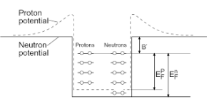
When metal is at T0, the wave function of valence e¯’s of all atoms in a metal overlaps each other. The e¯s cannot escape the atom, so they are trapped in a finite potential well. This overlapped region is called “Fermi Gas”, and since we assume it to be a gas, the e¯’s can be assumed as particles of an ideal gas. The classical approach tells us that at T0, all the e¯s have Ek=0.
So they all must occupy the same quantum state at T0, but Sir Pauli’s Exclusion Principle contradicts this approach(no two e¯ can have a set of identical quantum numbers, ever!). When the temperature is decreased to T0, all the lowest possible energy states will be filled, with each level containing max. of 2 e¯. The last possible energy state to be filled by e¯ is termed as “Fermi Energy”.
Fermi-Dirac Cone
Another unique property that graphene possesses is Fermi-Dirac Cone(it has at least a ton of unique properties). This is not rocket science, its easy to understand. If the energy of e¯ is expressed as a function of their momentum, we get parabolas for metal(partially filled) and insulators(bottom parabola filled with a band-gap). But Graphene has got something up his sleeve this time too.
Starting with Kinetic Energy equation and modifying it:
E = mv2, E= (mv)2/
, E = p2/2m; which suggests that energy and momentum have a quadratic relation and forms a parabolic graph. Surprisingly, graphene forms a cone instead of a parabola.
E= pv; suggesting that the e¯ move at a constant velocity just like photons and behave like massless particles.
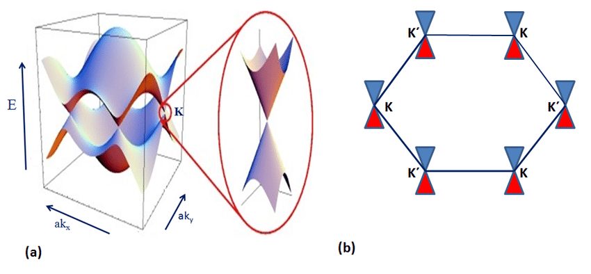
In the above picture of TBG, depicting the 3-D band structure of the system. The points of contact of both the curves are called Dirac Points where the Dirac cones are located.
The Real Physics At Play
Now that we are up to speed with the terminology, we shall explore the phenomenon at hand. In the BLG system, a Moiré pattern is developed when twisting occurs. Just like putting two thin sheets of plastic on one another and rotating the top layer keeping bottom fixed. This pattern forms small zones called Mini-Brillouin zones. The corners of the Brillouin zone have a Dirac cone attached to each of them. When the system is twisted these cones come closer and interact with each other, at nearly the MA the cones become Flat!
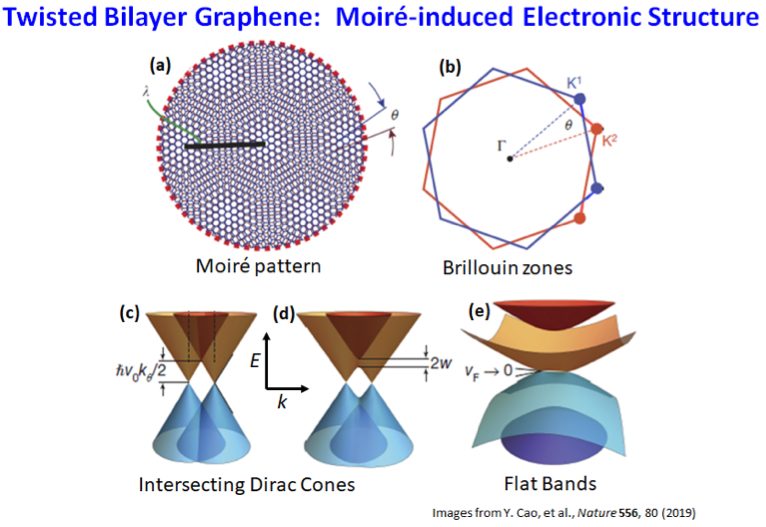
[Image: Crommie Research Group]
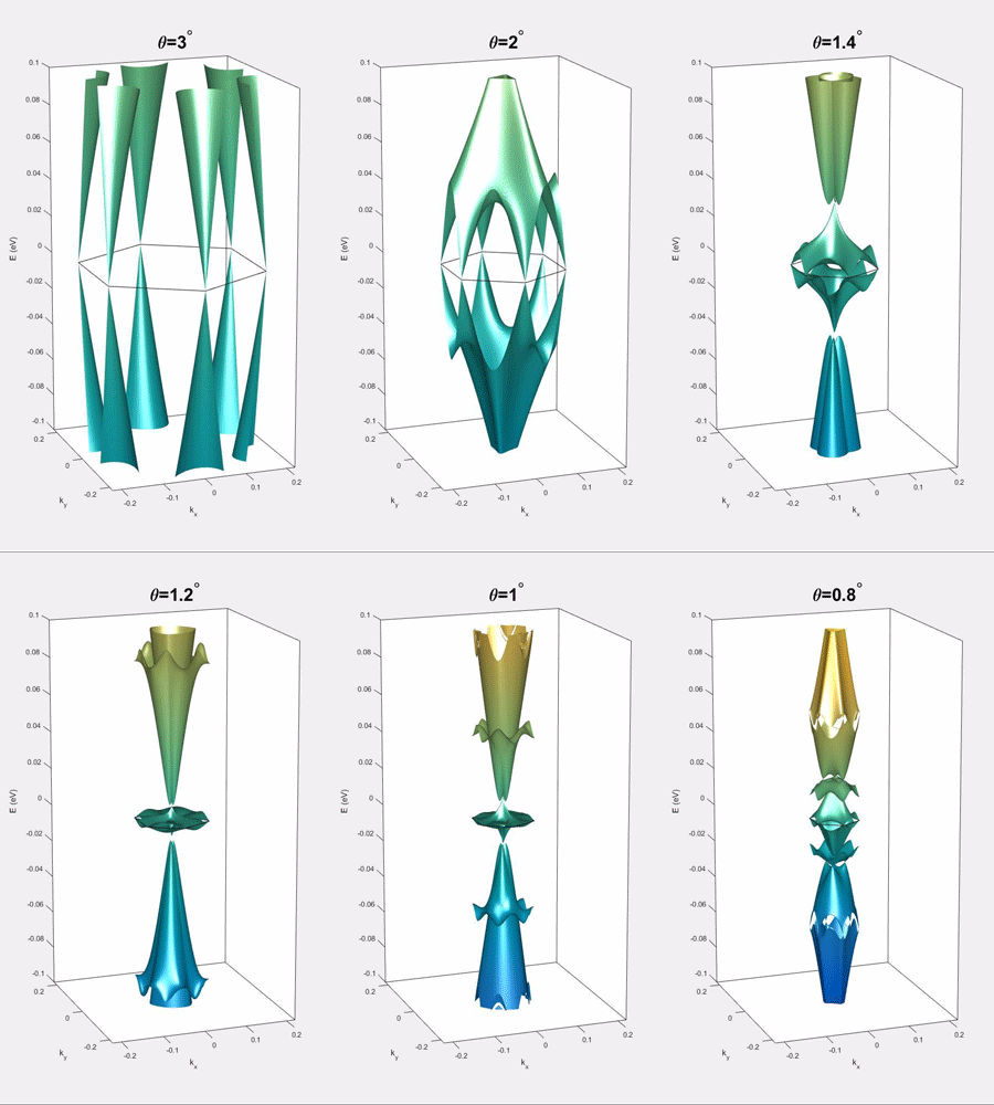
As a consequence of this, the Fermi Velocity drops to nearly zero, and so does the Fermi energy at charge neutrality point. The main catch here is the HFB, which stops the system from being a superconductor. At about 4k the system transitions from metal to an insulator(very unusual transition).
Furthermore when you, apply a Magnetic field(parallel or perpendicular) the system transitions from an insulator to metal. At the molecular level in the HFB system, the e¯s exist in form of spin-singlets. The application of the magnetic field results in the polarization of these singlets, leading to the Zeeman splitting which closes the gap and starts conduction.
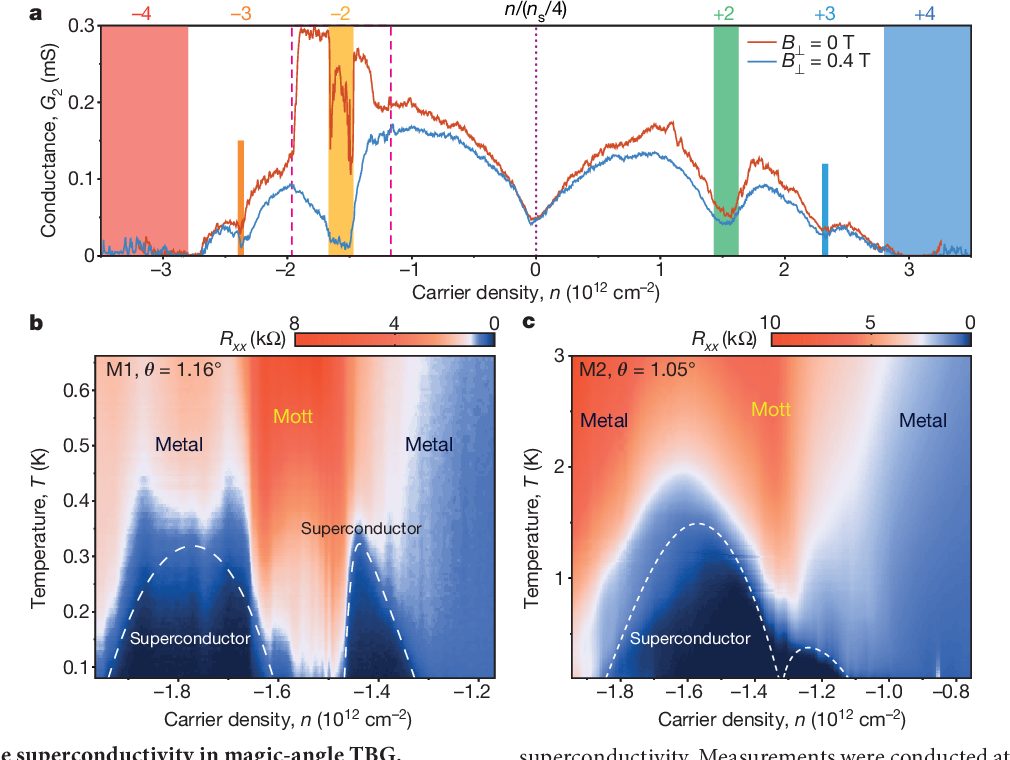
b) Four probe resistance measured at densities bounded by pink region, showing two SC domes are clearly visible next to Mott insulation state. The remaining region is labeled as metal. Highest TC = 0.5k. c) A similar plot for M2 (MA=1.050) is plotted with the highest TC = 1.7k. [Image: arVix.org]
Observing the graph of conductance vs charge-density, near -2e¯ an enhancement in conductance was detected, signaling the onset of superconductivity.
World Of Tunable Physics
The behavior of MA-TBG is beyond the explanation of weak coupling BCS theory, indicating strong electron correlations. The critical temperature: TC at which it occurred is 1.7k, highest among the known High TC superconductors. Also, the fact that the whole system can be controlled by applying gate-voltage, pressure, and controlling the DOS.
This experiment sure opens a new platform for highly tunable superconductors and hopefully, we will be able to use the technology in the future. But on the bright side, Graphene is being used to create a new class of Flexible Electronics, de-salination films and much more.
Sometimes, the simplest of the materials exhibit the most extraordinary properties.
RDX


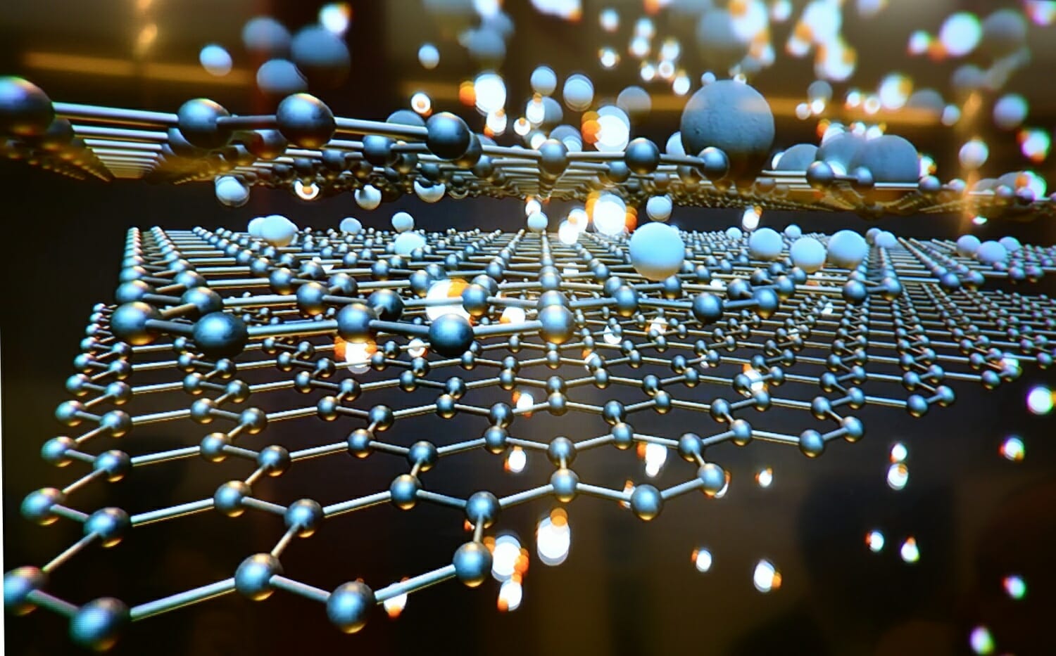

“Sometimes, the simplest of the materials exhibit the most extraordinary properties.”
True that.
Amazing citations, by the way.
Really very nice articles . The things are explained in a very perfact way . Really useful.
Thank you for your compliments, it inspires us to write more lucid articles.Hope you will continue reading.