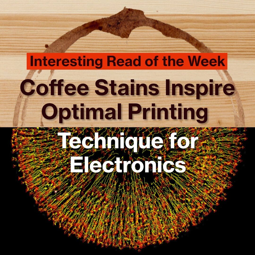
Once in a lifetime each of us have spilled coffee on our desk or workplace or at any other table. It creates a coffee stain, which everybody wipes out, thinking of nothing. But these coffee-stains develop because one of the most puzzling phenomena of Fluid Mechanics. This was called to be the “Coffee-ring Effect”. The same thing happened with Cambridge, Durham and Beihang University researchers and they produced most innovative concept of printing for fabrication of electronic devices. This effect, enabled the low-cost manufacturing of electronics with the help of coffee stain inspired printing technique. Some of these electronics are sensors, light detectors, batteries and solar cells, from Ink-Jet technological innovation.
Before going further, lets briefly know what is this puzzling “Coffee-Ring effect”.
The “Coffee-Ring Effect”:

Don’t get confused if you can’t understand the picture (its technical 😊). Simply we can say that, the liquid at the edges evaporates faster than on the inner side. This rapid evaporation induces flow inside droplet due to difference or gradient in surface tension (this can be observed in above figure at last). It is know as Marangoni Flow. Because of this, free surface at the edges get collapsed and liquid is trapped from the inner side of coffee stain. This flow induced towards the edge, carry almost all dispersed material rapidly at the final stage of drying process.
With this, if there is interaction of suspended particles of droplets with its surface, then only this effect is observed. At top of figure, inverted optical micro-graph of dried inkjet droplets on clean glass. Thus, in one line, it can be said that, coffee stain rings form because solid particles accumulate after the quicker evaporation of liquid from edges (this can be observed in middle part of above figure, with example of butanol).
Application in coffee stain inspired optimal printing solution:
Now knowing what is the phenomena of printing technique for electronics, lets understand how its done. Researchers observed that while printing on hard surfaces, inks accumulate at the edges creating uneven surfaces and irregular shapes. This damages whole printing process. But one thing noted here was, this was the same behavior as observed during the formation of coffee stains. This led into deep study on physics of ink droplets. It was done by combining particle tracking in high speed micro-photography, fluid mechanics, and different combination of solvents. Many conclusions, trial and errors, confirmations were made based on that study.
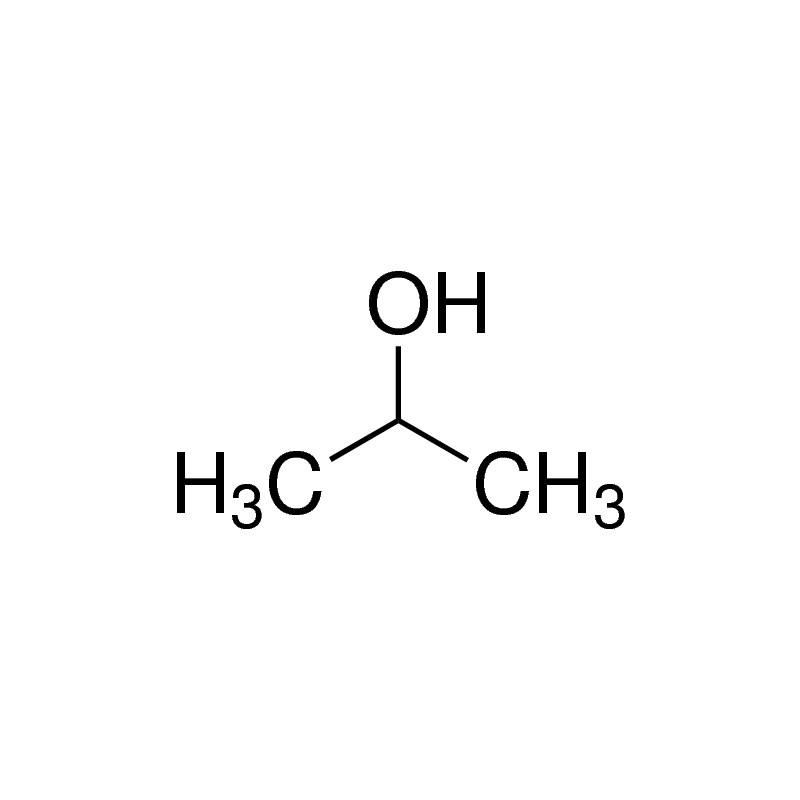
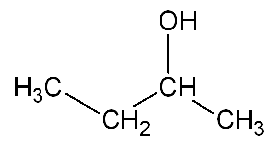
But among those, they prepared a solution/mixture of alcohol. To be specific, it was a solution of isopropyl alcohol and 2-butanol.
When mixture of these compounds was used, it was observed that ink particles distributed evenly across the droplet. Meaning, they also have shown coffee-ring effect, but in a systematic and even manner. Unlike the usual inks used in inkjet printers, they didn’t spread unevenly. But accumulated systematically, providing properly printed smooth surface even at edges. This led to coffee stain inspired optimal printing technique for fabrication of electronics.
One of the researchers said that, “The natural form of ink droplets is spherical — however, because of their composition, our ink droplets adopt pancake shapes.” This helped them to fabricate the printing electronic devices like sensors, photo-detectors, wearables, spray printing and many such inkjet printed devices.
They also observed that while drying these new ink droplets they deform across the surface smoothly. This leads to even spreading of particles and increases consistency. Along with this, they also avoid the addition of commercial additives like surfactants and polymers. This makes them more environment friendly and cheaper to get. Thus, with most common phenomena neglected by almost everyone, they made most efficient way of printing technique for fabrication of electronic devices.
Advantages of this printing technique inspired from coffee stain:
The coffee stain inspired printing technique has laid upon the foundation of high-speed additive manufacturing of all printed sensors. At the same time, it also helped large scale fabrication of systems requiring huge amount of large-scale integration.
Inkjet printing of such 2D-crystals enables scalable device fabrication. This device fabrication can be achieved with high consistency and reproducible properties.
Further, when this mechanism can be understood, more solvents can be adapted to opt for more applicability. This increases the acceptance of the technology in wider areas and more industrial reach can be obtained.

Also, it is now applicable in the areas of 2D crystals, nano-particles, organics and other different material platforms. Just now fabrication of complex devices is tough and costly. This technology can provide reliable printing of wide range of optically and electrically active materials and their mixtures. With that, there can be boost in production of complex emerging devices and at subsequently low costs.
This technology also has shown excellent consistency, scalability and reproducibility. Previously, printing of few hundred devices was considered success even with uneven behavior. But, this newest technology can be opted for the printing of electronic devices on silicon wafers or plastics.Using this technology, researchers have manufactured nearly 4500 identical devices on silicon wafer and plastic substrate. With more and more demand for printed devices in the market, current manufacturers are not able to fulfill needs. Usage of this technology enables them to scale-up inkjet printing of all kinds of 2-D crystals. Which means that, in future, needs of market can be matched easily at cheaper costs.
Future scopes:
Researchers expect sooner and reliable application of technology for industrial purposes. Their technology can be considered a game-changer and help companies and industries to grow in the field of printed devices.
Some of the successful attempts for the application of this technology are printed sensors and photo-detectors. They have shown promising results in terms of sensitivity and consistency. Naturally, with these results, future of printed and flexible electronics will be flourished. This is because, coffee stain printing technique provides results exceeding the current industrial needs yet are low cost and efficient. This perfectly makes them suitable for electronics industry.

In short, with this technology, dreams of smart cities will come true, at a way cheaper and yet inexpensive manner. Lastly one can say that, this innovation is best example of creation of most useful technology from most ignored stain of everyone’s life.
So next time in your life, you better not wipe your stains out.
— OSD


Informative article. Nice to read that it’s applications are so many.
On the other hand, I read an article about Scientists from university of Germany. They also tackled the effect but used dendrites in their study producing astonishing Results. Their developed formula can be easily mixed with today’s ink jet dye and used at very low cost. And have visible advantage over technique mentioned in this article.
I have attached the link here of this article.
https://www.rsc.org/news-events/journals-highlights/2018/sep/coffee-ring-effect/
Thank you for the review. This recommended article is pretty nice too. Still, bases and approach of both methods are different, due to which they both have their own pros and cons. Neverthless, both do will help emerge new possibilities and oppotunities for electronics. Do share and subscribe for similar stuff. Stay updated. Stay safe.